What is Copper Dry Etching and Its Benefits for Global Buyers?
Copper Dry Etching is a crucial process used in semiconductor manufacturing and microelectronics. This technique enables precise patterning on copper surfaces, which is essential for the development of advanced electronic devices. According to a recent MarketsandMarkets report, the global dry etching equipment market is projected to reach $8.1 billion by 2025. This growth signals a rising demand for efficient etching processes, particularly for applications involving copper components.
The benefits of Copper Dry Etching extend beyond just accuracy. It reduces material waste significantly when compared to traditional wet etching methods. This efficiency not only lowers production costs but also aligns with sustainability goals in the electronics sector. As companies strive to enhance their manufacturing processes, reliable data emphasizes that integrating Copper Dry Etching can improve yield rates by up to 30%.
Yet, there are challenges. Achieving optimal etching results requires precise control over process parameters. Variations can lead to inconsistencies, demanding continual innovation and adaptation. Overall, understanding Copper Dry Etching and its implications is vital for global buyers aiming to stay competitive in an evolving market landscape.
Understanding Copper Dry Etching Process and Techniques
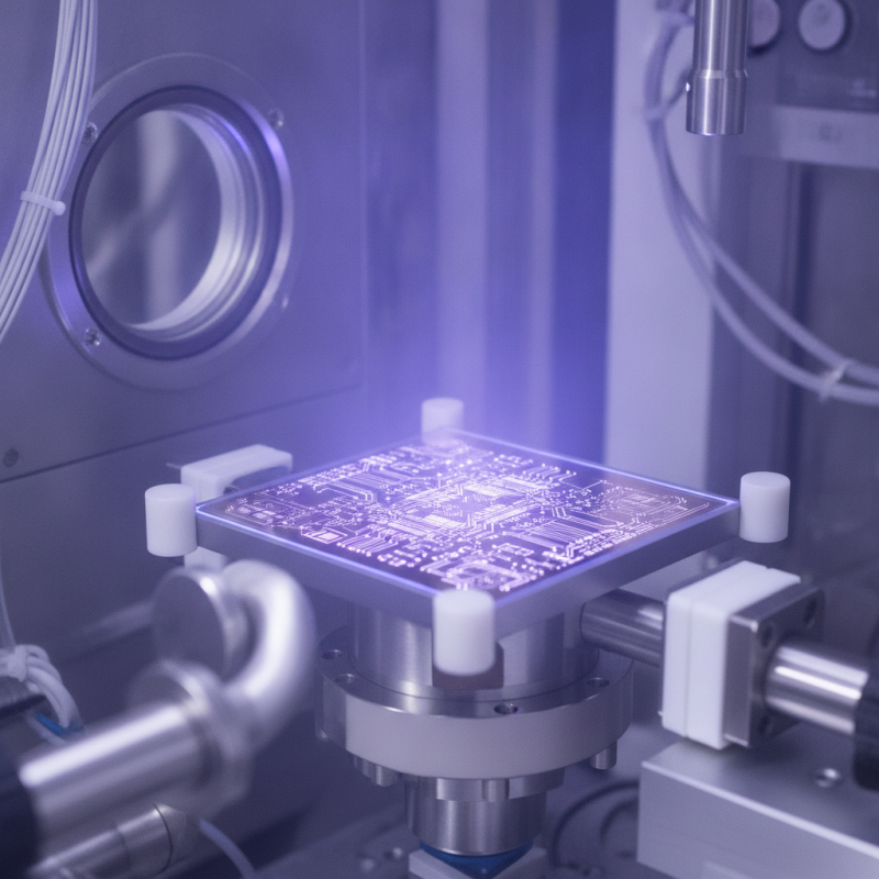
Copper dry etching is critical in semiconductor manufacturing. It is a plasma-based technique that removes material from copper surfaces. The process employs gases like chlorine or fluorine to create reactive ions. These ions effectively etch away copper with precision while maintaining the integrity of the underlying materials.
Research indicates that copper dry etching techniques have improved significantly over the past decade. According to a report from SEMI, the copper etch market will grow at a CAGR of 8% from 2021 to 2026. This growth reflects the rising demand for smaller, more efficient chips in consumer electronics. Companies are focusing on refining their dry etching methods to enhance resolution and reduce defects in copper layers.
Challenges remain in the process. Variability in etching rates can lead to inconsistent results. Achieving uniformity is crucial, particularly in advanced node technologies. As the industry pushes towards 5nm and beyond, the need for precise etching becomes paramount. Research continues to address these issues, but the path to perfection is ongoing.
What is Copper Dry Etching and Its Benefits for Global Buyers?
| Parameter | Description | Benefits |
|---|---|---|
| Process Type | Dry etching using plasma technology | High precision and minimal material loss |
| Applications | PCB manufacturing, semiconductor fabrication | Versatile usage across electronics industries |
| Environmental Impact | Lower chemical usage compared to wet etching | Reduced environmental footprint |
| Cost Efficiency | Optimized for large-scale production | Reduces overall production costs |
| Quality Control | Real-time monitoring and adjustments | Ensures high quality of etched features |
Key Benefits of Copper Dry Etching for Manufacturers and Buyers
Copper dry etching is a critical process in modern manufacturing. This technique ensures precise patterning of copper layers in various electronic components. It effectively removes the excess material while maintaining the integrity of the desired design. As a result, manufacturers can create more intricate and functional devices, meeting the rising demands of technology.
For global buyers, the benefits of copper dry etching are substantial. One key advantage is the enhanced precision. The method achieves tight tolerances that are essential for high-performance electronics. Additionally, it reduces material waste, contributing to a more sustainable production process. Without careful control, waste can escalate. This process minimizes such pitfalls.
Moreover, copper dry etching provides excellent reproducibility. Once the parameters are set, the process can consistently deliver high-quality results. Manufacturers often face challenges maintaining uniformity. This technique aids in overcoming those hurdles. The need for adaptability is apparent, yet the reliability of this method can significantly boost operational efficiency. It creates a pathway for innovation in new designs and applications.
Applications of Copper Dry Etching in Various Industries
Copper dry etching is a crucial process in various industries, particularly in electronics and semiconductor manufacturing. It allows for precise patterning of copper layers in printed circuit boards (PCBs) and integrated circuits. According to industry reports, the global PCB market size was valued at approximately $61 billion in 2022 and is expected to grow significantly. This growth partly results from advancements in copper dry etching technologies, which enhance the efficiency and accuracy of circuit designs.
In the automotive sector, copper dry etching plays a vital role. This process helps in creating intricate designs in sensors, which are essential for electric and autonomous vehicles. The demand for such technologies is projected to rise, with the electric vehicle market estimated to reach $800 billion by 2027. However, challenges remain. The need for complex architectures often outstrips current etching capabilities, leading to a constant push for innovation.
Moreover, the aerospace industry benefits from copper dry etching for lightweight, reliable components. In aerospace applications, even minor failures can be catastrophic. There is a growing emphasis on quality and precision, which puts pressure on manufacturers to refine their etching processes continuously. It's a balancing act between innovation and reliability, constantly pushing the envelope while reflecting on possible improvements.
Comparative Analysis: Copper Dry Etching vs. Traditional Etching Methods
Copper dry etching represents a significant advancement over traditional etching methods. Unlike wet processes that involve chemical baths, dry etching utilizes plasma to remove material. This technique enhances precision, leading to better pattern fidelity. According to recent industry reports, dry etching achieves critical dimension control within 5% variance, outperforming wet etching, which can exceed 10%. This precision is essential in the semiconductor industry, where miniaturization demands strict adherence to specifications.
Cost efficiency is another pivotal aspect. Dry etching reduces the need for hazardous waste management associated with wet etching. A study indicated that companies adopting dry etching can potentially cut their operational costs by 30%. However, the initial investment in dry etching equipment can be substantial, which raises questions about long-term viability for smaller firms.
Additionally, dry etching processes can sometimes yield non-uniform results in certain materials. This inconsistency may trigger challenges in scaling production. As the industry moves towards adopting copper dry etching, these potential pitfalls need addressing. Stakeholders must weigh options carefully before making a shift, ensuring their processes align with both budgetary constraints and quality standards.
Future Trends and Innovations in Copper Dry Etching Technology
Copper dry etching technology is rapidly evolving. As manufacturers seek more efficient methods, new techniques are emerging. This innovation includes advances in etching equipment and processes. These improvements aim to enhance precision and reduce waste, making copper dry etching more sustainable. The focus on environmental impact is increasingly crucial for global buyers.
Emerging trends indicate a shift towards automation and AI integration in dry etching systems. This technology promises easier process control and improved yields. Additionally, nanostructuring is gaining traction, allowing for intricate designs at smaller scales. However, challenges remain, particularly around cost-effectiveness and equipment maintenance. Companies must balance innovation with economic viability.
Customer preferences are changing as demand for customizations grows. Flexibility in processes is essential. This trend pushes manufacturers to adopt agile methodologies. Yet, the rapid pace of innovation can overwhelm established practices. Companies need to reevaluate their strategies continuously. As copper dry etching advances, buyers must stay informed to harness its full potential.
Copper Dry Etching Trends and Innovations
This bar chart illustrates the projected market demand for copper dry etching technology from 2021 to 2025. As seen, the market is expected to experience steady growth, indicating increasing relevance for global buyers.
Article Source:
NORTH EASTON MACHINE • 218 Elm Street • North Easton, MA 02356 • 508-238-6219

